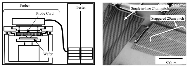
The probe card is the key tool used at "wafer test" to check quality of LSI devices. A schematic diagram of a wafer test system is shown in Fig.1. In the test process, to establish electrical contact between LSI chips developed on a wafer and the tester, needle probes are applied directly on the electrodes of the LSI chips. The printed wiring board equipped with probes, used in this process, is the probe card. For probe cards, increasingly miniaturized and sophisticated semiconductor devices necessitate the establishment of a probing technology adapted to small-pitch, high-density electrodes. According to ITRS 2006, for example, it is expected that single in-line, 20 ![]() m-pitch wire bonding will be achieved in 2009 and call for probing of electrodes 10
m-pitch wire bonding will be achieved in 2009 and call for probing of electrodes 10 ![]() m to 15
m to 15 ![]() m in width for wafer testing (Semiconductor Industry Association & SEMATECH, 2006). Furthermore, since low-k films and the CUP (circuit-under-pad) structure are becoming widely used, permissible mechanical stress of semiconductor devices is decreasing. Consequently, probe cards need to meet an important requirement to reduce contact force. To fulfill these requirements, making use of MEMS technology, a probe module of cantilever type using build-up process was proposed by authors. On this probe module, it was reported that it features high probing position accuracy and low force for contacting Au-plated wafers (T. Ishida, et al, 2007). To put this module to practical use, it is additionally necessary to verify that the probes exhibit adequate mechanical durability in actual use. Furthermore, with most semiconductor devices, electrodes are made of Al sputter film, and therefore stable contact with Al film must be ensured. In these regards, the module's mechanical durability was evaluated and basic analyses of contact with Al film were conducted.With higher integration of semiconductor device, the pitch and the size of electrodes on device become smaller and smaller. In response to this trend, the probing technology for LSI testing device is needed to be more sensitive. Besides, it is necessary to establish contact with electrode under low contact force, since the mechanical stress tolerance for probing become smaller. Moreover, removing the surface oxide layer of Al by scrubbing the probe is needed for achievement of ohmic contact with Al electrodes under low contact force.
m in width for wafer testing (Semiconductor Industry Association & SEMATECH, 2006). Furthermore, since low-k films and the CUP (circuit-under-pad) structure are becoming widely used, permissible mechanical stress of semiconductor devices is decreasing. Consequently, probe cards need to meet an important requirement to reduce contact force. To fulfill these requirements, making use of MEMS technology, a probe module of cantilever type using build-up process was proposed by authors. On this probe module, it was reported that it features high probing position accuracy and low force for contacting Au-plated wafers (T. Ishida, et al, 2007). To put this module to practical use, it is additionally necessary to verify that the probes exhibit adequate mechanical durability in actual use. Furthermore, with most semiconductor devices, electrodes are made of Al sputter film, and therefore stable contact with Al film must be ensured. In these regards, the module's mechanical durability was evaluated and basic analyses of contact with Al film were conducted.With higher integration of semiconductor device, the pitch and the size of electrodes on device become smaller and smaller. In response to this trend, the probing technology for LSI testing device is needed to be more sensitive. Besides, it is necessary to establish contact with electrode under low contact force, since the mechanical stress tolerance for probing become smaller. Moreover, removing the surface oxide layer of Al by scrubbing the probe is needed for achievement of ohmic contact with Al electrodes under low contact force.
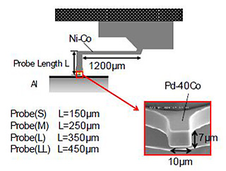
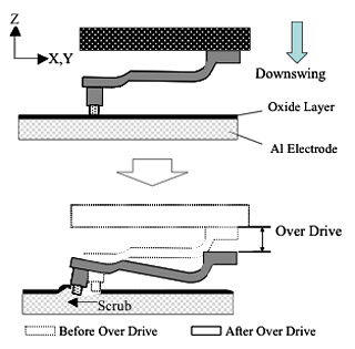
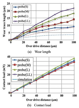
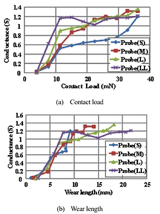
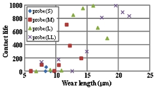
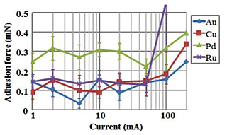
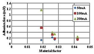
The aim of the present research is to investigate the effect of probe morphologies on the achievement of ohmic contact by lower contact force. In this work, as shown in Fig.2, MEMS probes with different probe length were prepared and the contact characteristics of MEMS probe with Al electrode were investigated by using the contact machine shown in Fig.3. Figure 4 shows the effect of probe length on wear length and contact load. It was confirmed that the longer probe length enables the longer wear traces of Al substrate while the contact force is almost identical for the same over drive distance. Fig.5 shows the effect of contact load and wear length on conductance between probe and Al substrate. It is obviously confirmed that longer probe enables the ohmic contact with Al by lower contact force and that the wear length is a important factor to achieve ohmic contact. Fig.6 shows the relationship between wear length and contact life, which the number of contact when contact conductance reaches zero. It was confirmed that longer wear length and longer probe length increase the contact life although there is an optimum vale for them. The main reason to cause contact failure is the sticking between contact tip of probe and worn debris of Al substrate. Thus, It may be assumed the material with higher hardness and lower adhesivity with Al is desired for the contact tip material. In order to prove these hypotheses, adhesion force with Al was measured for the various metals at different current charged. Fig.7 shows the effect of current on adhesion force of each metal.for materials of contact tip. It was confirmed that adhesion force hardly changed at a lower current but when the current exceeds cirtical value the contact force rapidly increased. The reason is considered to be due to the melting of each metals at contact points. Thus, to suppress the melting at the contact points, contact material should be designed to have higer thermal conductivity, lower electric resisitance and lower hardness. Figure 8 shows the effect of material factor, which is the value of thermal conductivity divided by resistance and hardness, on the adhesion force. As shown in Fig.8, there is a clear relation between adhesion force and material factor and it is confirmed that material witg higher material factor, such as Cu is suitable for the contact tip material.